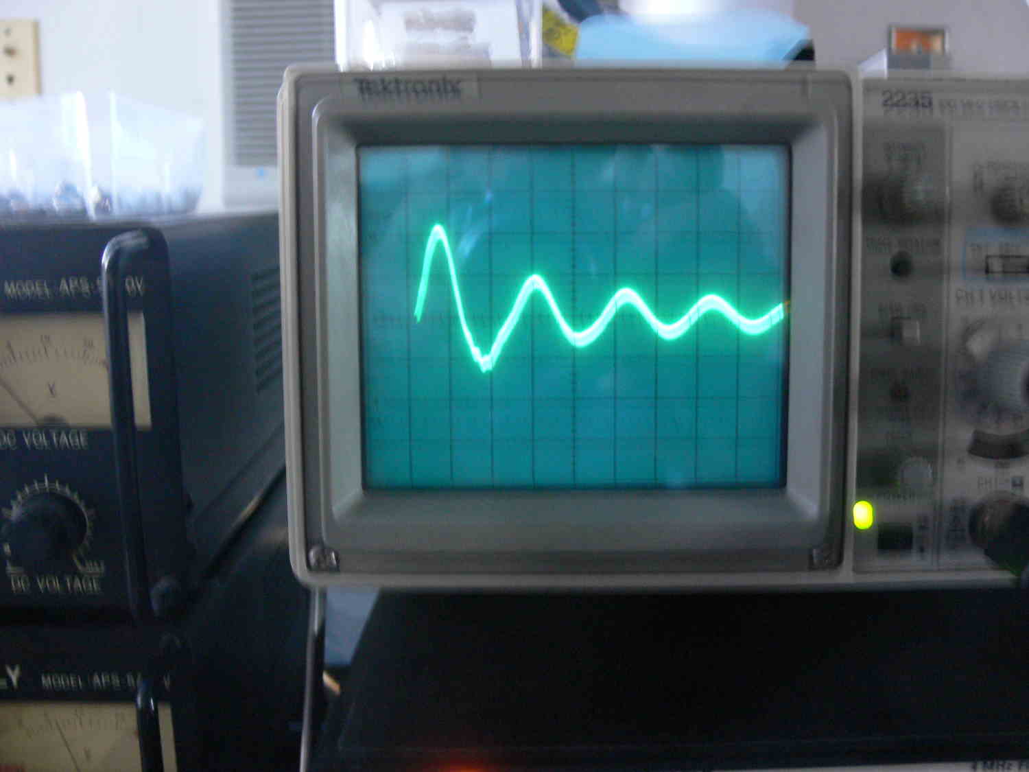
It works! This is the modular HV power supply for the modular CD
ignition. Everything from one power supply and one CD module per
spark plug down to one power supply per engine and one waste spark
coil per rotor.
Thanks to all the smart people on here that have helped. Thanks to my
wife Robin for putting up with my 16 hour a day work habits :)
It has been a mount Everest learning curve.
The IGBT is running at about 80 F and the input voltage for the power
supply is 8 volts for the scope picture shown.
With no load input current is less than a tenth of an amp.
The scope is set to 50 volts per division so what you are seeing is
350 Volts peak. That varies with pulse width and output current will
vary with frequency.
The time base is 10 usec per division.
The osc is running at 40Khz.
The IGBT is the same one I am using in the CD ignition modules. The
coil is the same one Lin Tech uses.
The idea here is to use a sledge hammer IGBT.
Parts cost less the PC board is less than $20. No tricky, expensive
and troublesome LSI chips :) CMOS 555's and 4050's are less than $1
All this is initial. Pulse width is manually adjustable as is the
frequency.
I am very relieved. It has been looking bad and too hard to do for
years.
Paul Lamar
Excellent effort Paul! It appears that you have finally achieved your
goal of a practical CD system. I'm sure there are many tests to run and I
assume the results will confirm your initial findings. This is exciting
news!
Gary Knutson
Yes I agree! Very exciting. It has been running on the bench for five
hours so far. I will eventually put it in the oven and cook it at 200 F :)
I always thought MSD was charging too much :)
Paul Lamar
Paul
Did that sense res on the Lin Tech pcb fail or overheat?
The waveform to expect will be a linear ramp starting at 0 and
increasing in the + direction as switch on time progresses. If you see
an exponentially rising waveform it indicates saturation of the xfmr.
The saturation current of your xfmr is 20A. What do you see for voltage
spikes on the collector?. What is the pn of the fet in the Lin Tech
pcb? BTW an IGBT is not the best device for low Vdc input. It has a
Vsat of 2V or so. The mosfet is the preferred device to use here as the
Lin Tech design. Also the proto board altho convenient is prone to
parasitic inductance effects in hi current switch ckts. If possible re
construct the ckt using copperclad with short paths for the power device
and the gate drive ckt. A series res about 5-10 Ohms in the gate-drive
path is usually used to damp potential parasitics with mosfets.
Robert
Yes it did.
Here is the spike on the collector. The scope is set to .2 usec per
division (yes 200 ns)
and 1 volt per vertical division. Hardly a problem. What is really
tricky about
these things is circuit board layout. You need super low inductance in
the high current switching circuits (HCS) and lots of capacitance on
the 12 volt
supply close to the HCS. This is why surface mount MOSFETs are used as they
can be placed on the back side of the transformer.
BTW this will run at well over 100Khz.
The MOSFET in the Lin Tech is a ST7846DP. I did not look up the specs.
If you
do please email them back. Here is the pdf on the Lin Tech board.
It is a relatively old design. Oct 2008. Ancient history in the world of
integrated
circuits :) You would not want a new computer built in 2008 would you? :)
Some advances in IGBT's have been made recently. These are late IGBT's.
Paul Lamar
The Rotary Engine News Letter. Powered by Linux.
ACRE NL web site.
http://www.rotaryeng.net.
You Tube
http://tinyurl.com/beqqxas.
Copyright 1998-2013 All world wide rights reserved.